The EDA work on the 84 Badge - Dev PCB
The development board was just a quick way to test out the electronics. So, I wanted to keep it a small and simple as possible to keep manufacturing costs to a minimum.
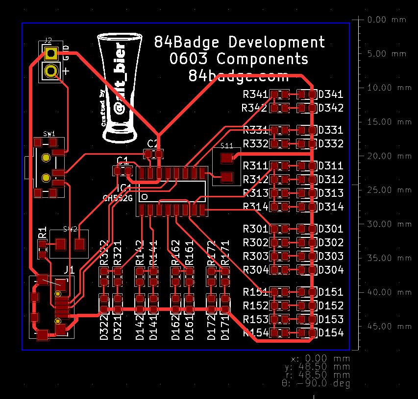
PCB Layout
As it turns out I was able to get all the components to fit into a 48mm (1.9in) square.
I was also able to get all the traces onto one layer so that no vias were required.
It was a tight fit but everything worked perfectly enough that I was able to move the electrical design to the prod project with no modifications.
This completes the Dev PCB review (it was simple so there was not much to review).
You can download a PDF of the Dev PCB file here.